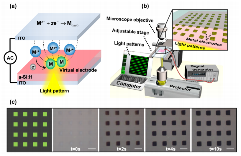
(a) Illustration of the mechanism for fabricating metal electrodes utilizing the opticallycontrolled digital electrodeposition (ODE) technique. (b) Illustration of the OEK experimental system for application of the ODE technique. (c) The computergenerated patterns and the corresponding silver electrodes fabricated on the chip’s surface.
Both semiconductor layers and metal electrodes are necessary components of micro/nano scale devices such as sensors, solar cells, and field-effect transistors. The ability to rapidly design and cost-effectively pattern micro metal electrodes along with semiconducting materials is vital for fabricating novel devices in micro/nano scale, and has attracted considerable attentions from researchers worldwide.
Direct patterning methods based on metal nano particle inks—such as screen printing, micro-contact printing, nano imprinting, inkjet printing, laser-induced printing, and electro deposition patterning have been found to be particularly useful in fabricating electrically conductive, micro-scale structures on a substrate. However, each of these methods has its own limitations.
In order to address these limitations of existing methods, researchers from Shenyang Institute of Automation (SIA), the Chinese Academy of Sciences (CAS) come up with a maskless rapid and bottom-up metal patterning method called optically-controlled digital electrodeposition (ODE). Compared to other method for patterning metal film, this proposed technique is capable of fabricating arbitrary, micro-scale, metal structures directly onto a semiconductor surface at room temperature and at atmospheric pressure conditions, while requiring no mask-based lithography process or metal nanoparticle inks. Moreover, utilizing this method, silver electrodes owning high electrical conductivity and arbitrary shapes were fabricated in a rapid speed. Furthermore, taking advantage of this method, micro/nano logic devices such as nanowire-based field-effect transistors could be assembled rapidly, and hence this method could potentially become an alternative, low-cost and flexible technology for fabricating integrated nano-devices in the future.
Through fabricating custom-designed, silver micro-electrodes rapidly without using a silver nanoparticle ink, conventional vacuum deposition techniques, or microlithographic masks, the researchers demonstrated the result. Micro-electrodes with customized geometries, high conductivity of 2 × 10⁷S/m and a smallest line width of 2.7 μm, were directly fabricated onto a substrate in a digitally controlled manner at atmospheric pressure and room temperature conditions.
To see more about the research, please refer to Optically-controlled digital electrodeposition of thin-film metals for fabrication of nano-devices, which is published on OPTICAL MATERIALS EXPRESS Vol. 5, 2015. This work was supported by the National Natural Science Foundation of China (Project No. 61302003), the NSFC/RGC Joint Research Scheme (Project No. 5141101088), the CASCroucher Funding Scheme for Joint Laboratories (Project No. 9500011), and the CAS-FEA International Partnership Program for Creative Research Teams.