Due to the potential application in nano-electronics, nanowires of metallic and semiconducting materials have drawn a great deal of interest from both academic and industrial domains. For instance, Cu nanowires can take the place of currently used copper wires and find promising application in integrated circuit. Because of the extensive use of copper materials in electronics, Cu nanowires, with special quantum characteristics, will find their broad applications in micro-nano electronics fields. CuO is a p-type semiconductor material with narrow bandgap energy of 1.2-1.5 eV at room temperature. It has been shown that CuO can be used in high temperature superconductors, magnetic storage media, gas sensor, field emitters and heterogeneous catalysis, and so on. The CuO nanowires based sensors can be taken advantage of testing many objects, such as NO2, H2S, pH, humidity, glucose, etc.
However, the efficiency of assembly for further fabricating nano-electronic device needs to be greatly promoted before the realization of extensive application. Although significant progress has been made in assembling nanowires, there is still no report about realizing large-scale assembly of Cu nanowires at one time. For solving the problem, researchers from Shenyang Institute of Automation (SIA), the Chinese Academy of Sciences proposed a method named Floating Electrical Potential (FEP) di-electrophoresis (DEP) and realized the large-scale assembly of Cu/CuO nanowires micro-electrode chip for the first time.
The experiments of large-scale assembly are carried out with assembly success rate evaluated by scanning electron microscopy (SEM). And in the testing experiments after the assembly, the researchers found by chance that some of the assembled Cu nanowires show field effect transistor (FET) characteristics, which means that due to nanowire’s extremely high surface-to-volume ratio and metal activeness at nano-scale, some Cu nanowires are oxidized in the air and turned into CuO nanowires which is semi-conduct. The experimental results show that this method can meet the requirement of high-efficiency assembly of Cu/CuO nanowires for further nano-electronic device fabrication and application
With the well-dispersed Cu/CuO nanowires and the micro-electrode chip, large-scale assembly experiments of the nanowires are performed. An AC DEP signal is applied to the source electrode and the gate electrode, with frequency 1.5MHz and peak-to-peak voltage 12V, which generated DEP force to actuate and assemble Cu/CuO nanowires at the micro-electrode gaps, and the DEP duration time is about 5s. After the assembly, the micro-electrode chip is rinsed in deionized water to remove the remaining surfactant and put into a dry oven to evaporate the water. And the experimental results are shown in Figure 1.
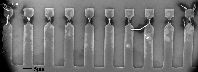
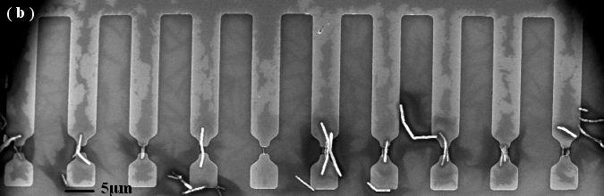

Figure 1 SEM images of Cu/CuO nanowires assembled on the micro-electrodes (Image provided by XU Ke et.al)
From Figure 1, it can be seen that Cu/CuO nanowires were well assembled between the source electrode and the floating electrode on each unit of ten electrode pairs, which is one typical representative of the assembly results on the whole micro-electrode pairs. According to the statistics results, the successful rate of the assembly is about 90%, which verified theeffectiveness and the efficiency of the large-scale assembly method. After the assembly, the electrical properties of some well-assembled nanowires are measured by Agilent4155C semiconductor parameter analyzer, and field effect transistor characteristics curves are found as shown in Figure 2.
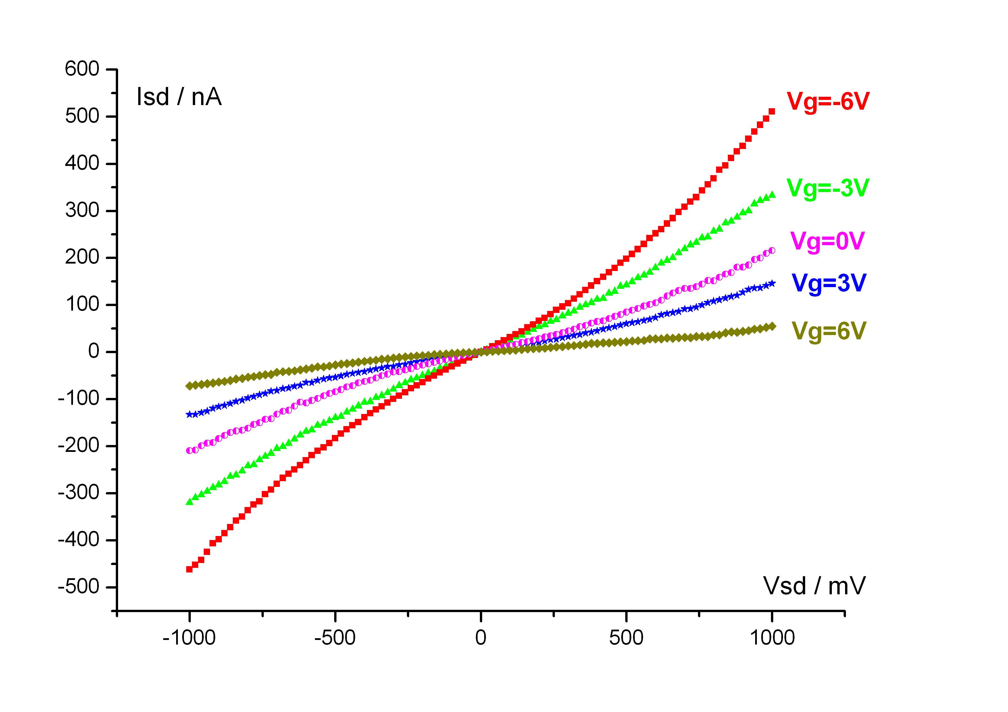
Figure 2 FET characteristics curves of CuO nanowire measured after the assembly (Image provided by XU Ke et.al)
From the electrical characteristics curves shown in Figure 2, it can be seen that the current between source and drain varies with the gate voltage changing, which shows obvious FET characteristics and thus verified that some Cu nanowires are actually oxidized to CuO nanowires and present semi-conductor characteristics.
This work was published on the Science China Technological Sciences, Volume 57, Issue 4, April 2014, 734-737. It was supported by the National Natural Science Foundation of China (Grant Nos. 51005230), China Postdoctoral Science Foundation (Grant No. 2012M520654).
Contact:
XU Ke
Shenyang Institute of Automation, Chinese Academy of Sciences
E-mail: xuke08@sia.cn