Micro-fabrication techniques to assemble composite devices based on electrically conductive polymers and carbon nanotubes (CNTs) have recently attracted the attentions of many researchers, due to their attractive chemical, electrical, and mechanical properties. Currently, there are many fabrication methods used for patterning polymer/CNT composites, such as photolithography, capillary molds, micro-contact printing, micro-transfer imprinting, and inkjet printing. However, each of these methods has self-limitations such as needs for complicated fabrication process, low resolution, high cost and so on, which restrict their further applications.
In order to address these drawbacks, the researchers from Shenyang Institute of Automation, the Chinese Academy of Sciences (CAS) propose a new technique for fabricating conductive polymeric electrodes based on a PANI/MWCNT composite utilizing an optically-induced electrokinetics (OEK) chip. This technology enables the rapid fabrication of polymeric electrodes with customizable geometries, without the use of any physical molds. Since computer-generated images are projected into an OEK chip to induce localized electrokinetics forces (see Fig. 1), we refer to this method as “digitally-controlled electrokinetics” (DCE). In this technique, the light patterns designed by the computer are projected on a-Si:H substrate and can work as located virtual electrodes. When there is an external AC signal exerted on the chip, the conductive polymer particles are moved to the electrodes and deposited to be electrodes which are formed by the conducting polymer and CNTs. Utilizing this technique, conducting electrodes with arbitrary geometries can be fabricated in 1-2 minutes without using any physical molds and complicated process.
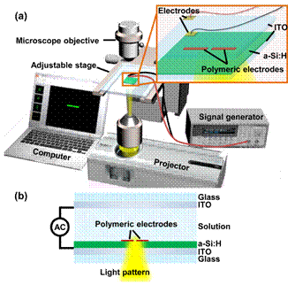
Fig. 1. (a) Illustration of the experimental system. (b) Illustration of the two-dimensional structure of the OEK chip (Image provided by LIU Na et.al)
The conducting electrodes have been characterized using SEM, as shown in Fig. 2. The fabricated electrodes were used to assemble micro-sensor for detecting ethanol. The capacity of the assembled sensor to detect ethanol has been demonstrated in Fig.3

Fig. 2. A SEM picture of the patterned polymeric electrodes utilizing the DCE technique. The scanned result shows that the polymeric electrodes are uniform and continuous, and the edge of the electrodes is clearly defined. (Image provided by LIU Na et.al)
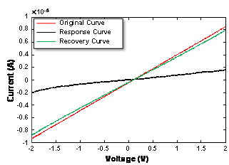
Fig. 3. The I/V curves of a pair of electrodes with MWCNTs bundles across the electrode gap. Each polymeric electrode is 150 μm of length, 30 μm of width, 2 μm of height. “Original Curve”, “Response Curve”, and “Recovery Curve” indicate the total resistance of the polymeric electrodes and the MWCNTs bundles under the experimental conditions of no ethanol present, immediately after exposure to ethanol, and 10 seconds after exposure to ethanol when the ethanol completely evaporated, respectively.(Image provided by LIU Na et.al)
This work was published on IEEE Transactions on Nanotechnology, Volume 13 March 2014 245-253. It was supported by the National Natural Science Foundation of China (Project code: 61107043, 61302003), the CAS-Croucher Funding Scheme for Joint Laboratories (Project No. 9500011) and the CAS FEA International Partnership Program for Creative Research Teams.
CONTACT:、
Liu Na
Shenyang Institute of Automation, the Chinese Academy of Sciences
Email: liuna@sia.cn